
A new method has been developed for production of silicon nanofbers by electrolysis from molten chloride-fluoride salts. Fibrous electrolytic deposits of silicon with fbers of various diameters (100 nm or less) and silicon crystals up to 20 nm in size on the average have been obtained.
Advantages
• Owing to smaller energy consumption, the production costs of silicon nanofbers are reduced by a factor of 1.5–2 as compared to the known methods;
• The new method makes it possible to control the properties of silicon fbers, attaining the surface structure that is optimal for specifc requirements.
APPLICATIONS
• Owing to their unique geometry, semiconductor silicon nanofbers have found application in nanoelectronics, biosensorics, and solar batteries-related technologies.
• Silicon nanofbers are used for making anodes of lithium chemical current sources. They withstand multiple recycling of lithium with 4-fold swelling and shrinkage without failure (unlike silicon macrosamples).
• The capacity of lithium chemical current sources with anodes made of silicon nanofbers increases 2 to 3 times as compared to the capacity of lithium chemical current sources with graphite anodes.
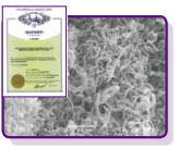
Fibrous silicon deposit obtained by refning of silicon from KCI-CsCI-K2SiF6 melt.
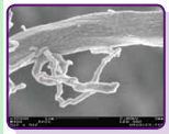
Silicon fbers of various diameters. Seen is the faceting of thick fber, which confrms the crystalline structure.